


Ahmedabad
(Head Office)Address : 506, 3rd EYE THREE (III), Opp. Induben Khakhrawala, Girish Cold Drink Cross Road, CG Road, Navrangpura, Ahmedabad, 380009.
Mobile : 8469231587 / 9586028957
Telephone : 079-40098991
E-mail: dics.upsc@gmail.com
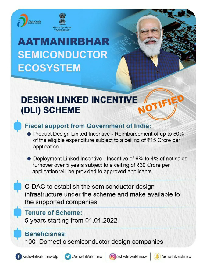
Design linked incentive scheme for Semiconductors
Context: The article is based on the news “The need to overhaul a semiconductor scheme” which was recently published in The Hindu.
What is the Design linked incentive scheme(DLI)?
• Design Linked Incentive Scheme offers financial incentives, design infrastructure support across various stages of development and deployment of semiconductor design for Integrated Circuits (ICs), Chipsets, System on Chips (SoCs), Systems & IP Cores and semiconductor linked design.
• Its primary aim is to cultivate semiconductor design capabilities in India, with the understanding that home-grown IP will organically evolve as local talent fosters the creation of indigenous companies over time.
• The Centre for Development of Advanced Computing, a scientific society operating under MeitY is the nodal agency.
What are the issues with the scheme?
• The Design Linked Incentive Scheme mandates that beneficiary start-ups maintain their domestic status for at least three years after receiving incentives, and for this they cannot raise more than 50% of their requisite capital via foreign direct investment.
• The funding landscape for chip start-ups in India continues to be challenging despite promising IP and business potential.
• The Design Linked Incentive Scheme has witnessed poor results and fewer participation.
• The relatively modest incentives under the Design Linked Incentive Scheme (capped at ₹15 Crore for Product DLI and ₹30 Crore for Deployment Linked Incentive, per application) would not make for a worthwhile trade-off for start-ups standing to lose out on access to crucial long-term funding.
Way Forward
• Any noticeable shortfall in investment for Design Linked Incentive Scheme beneficiary start-ups could be bridged by equity financing bringing in foreign funds.
• The scheme needs to be revised to focus on the broader objective of facilitating design capabilities for a wide array of chips within the country, so long as the entity engaging in the design development process is registered in India.
• Delinking of ownership from the development of semiconductor design and adopting more start-upfriendly investment guidelines is required. It is likely to boost their financial stability and assure them of global exposure.

Address : 506, 3rd EYE THREE (III), Opp. Induben Khakhrawala, Girish Cold Drink Cross Road, CG Road, Navrangpura, Ahmedabad, 380009.
Mobile : 8469231587 / 9586028957
Telephone : 079-40098991
E-mail: dics.upsc@gmail.com
Address: A-306, The Landmark, Urjanagar-1, Opp. Spicy Street, Kudasan – Por Road, Kudasan, Gandhinagar – 382421
Mobile : 9723832444 / 9723932444
E-mail: dics.gnagar@gmail.com
Address: 2nd Floor, 9 Shivali Society, L&T Circle, opp. Ratri Bazar, Karelibaugh, Vadodara, 390018
Mobile : 9725692037 / 9725692054
E-mail: dics.vadodara@gmail.com
Address: 403, Raj Victoria, Opp. Pal Walkway, Near Galaxy Circle, Pal, Surat-394510
Mobile : 8401031583 / 8401031587
E-mail: dics.surat@gmail.com
Address: 303,305 K 158 Complex Above Magson, Sindhubhavan Road Ahmedabad-380059
Mobile : 9974751177 / 8469231587
E-mail: dicssbr@gmail.com
Address: 57/17, 2nd Floor, Old Rajinder Nagar Market, Bada Bazaar Marg, Delhi-60
Mobile : 9104830862 / 9104830865
E-mail: dics.newdelhi@gmail.com