


Ahmedabad
(Head Office)Address : 506, 3rd EYE THREE (III), Opp. Induben Khakhrawala, Girish Cold Drink Cross Road, CG Road, Navrangpura, Ahmedabad, 380009.
Mobile : 8469231587 / 9586028957
Telephone : 079-40098991
E-mail: dics.upsc@gmail.com
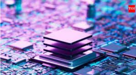
As part of its long-term vision to evolve into a global electronics powerhouse, the Government of India is set to unveil a new fund exceeding ₹1 trillion (approximately $10.8 billion) to bolster the domestic semiconductor ecosystem. This initiative, part of the newly launched India Semiconductor Mission (ISM) 2.0, aims to reduce critical import dependencies and secure high-tech supply chains. The fund is designed to transition India from assembly-level operations toward advanced \'wafer fabrication\' and indigenous chip design, targeting 2- nanometre (nm) and 3-nm technology nodes by the early 2030s. • Financial Outlay and Timing: The proposed ₹1 trillion fund is expected to be officially launched within the next two to three months, building upon the initial ₹76,000 crore incentive program (ISM 1.0) introduced in 2021. • Expansion of Incentive Scope: Unlike the previous phase, which primarily focused on assembly and testing (ATMP), this fund will provide massive subsidies for chip design projects, high-end manufacturing equipment, and upstream raw material supply chains. • Focus on Advanced Technology: A primary objective of this new capital injection is to move India up the value chain toward sub-28nm chip fabrication, aiming for capabilities comparable to global leaders like Taiwan and South Korea by 2032. • Incentivizing the \'Fabless\' Ecosystem: The fund aims to support at least 50 domestic \'fabless\' companies (firms that design but do not manufacture chips) by expanding the Design Linked Incentive (DLI) scheme, fostering local Intellectual Property (IP). • Geopolitical Resilience: By mirroring global initiatives like the $52 billion US CHIPS Act, India seeks to insulate its AI, smartphone, and automotive industries from West Asian disruptions and global supply chain volatility. • Integration with State Policies: The central fund will work in tandem with state-level policies (like those of Gujarat and Uttar Pradesh) to offer combined capital assistance of up to 70-80% for mega-projects. Key Definitions • Semiconductor Fabrication (Fab): A factory where integrated circuits (chips) are manufactured. It is one of the most capital-intensive and technologically complex industrial processes. • Fabless Company: A semiconductor company that designs and sells hardware and chips but outsources the actual fabrication to a third-party foundry. • Design Linked Incentive (DLI): A financial support scheme specifically for the design and development of semiconductor IPs, targeting startups and MSMEs. • Integrated Circuit (IC) Layout-Design: The three-dimensional arrangement of the elements and interconnections that make up an integrated circuit. Constitutional & Legal Provisions • Union List (Seventh Schedule): Under Entry 52 (Industries, the control of which by the Union is declared by Parliament to be expedient in the public interest), the Central Government holds the primary authority to regulate and fund the semiconductor sector. • Semiconductor Integrated Circuits Layout-Design Act (SICLDA), 2000: This is the primary legal framework for Intellectual Property Rights (IPR) in the chip industry, ensuring that original 3D designs are protected for a period of 10 years. • National Policy on Electronics (NPE), 2019: The overarching policy framework that envisions India as a global hub for ESDM (Electronics System Design and Manufacturing). • Automatic Route (FDI): Under current FDI norms, 100% foreign investment is permitted in the semiconductor sector through the automatic route to encourage global majors like Micron and TataPSMC. Conclusion The announcement of this $11 billion fund marks the transition of India\'s semiconductor strategy from \'foundational\' to \'expansionary.\' By focusing on the entire value chain—from specialized chemicals to advanced IP design—India is attempting to bypass the \'middle-income trap\' of being just a low-end assembler. However, the success of this mission will depend on the speed of administrative approvals (the 60-day window) and the consistent availability of ultra-pure water and uninterrupted power, which are the lifelines of any fabrication unit. UPSC Relevance • GS Paper III: Issues relating to planning, mobilization of resources, growth, and development; Science and Technology- developments and their applications and effects in everyday life. • GS Paper II: Government policies and interventions for development in various sectors and issues arising out of their design and implementation. • Prelims: Key statutory acts like SICLDA 2000, definitions of Deep Tech, and the role of the Ministry of Electronics and Information Technology (MeitY) in the India Semiconductor Mission.

Address : 506, 3rd EYE THREE (III), Opp. Induben Khakhrawala, Girish Cold Drink Cross Road, CG Road, Navrangpura, Ahmedabad, 380009.
Mobile : 8469231587 / 9586028957
Telephone : 079-40098991
E-mail: dics.upsc@gmail.com
Address: A-306, The Landmark, Urjanagar-1, Opp. Spicy Street, Kudasan – Por Road, Kudasan, Gandhinagar – 382421
Mobile : 9723832444 / 9723932444
E-mail: dics.gnagar@gmail.com
Address: 2nd Floor, 9 Shivali Society, L&T Circle, opp. Ratri Bazar, Karelibaugh, Vadodara, 390018
Mobile : 9725692037 / 9725692054
E-mail: dics.vadodara@gmail.com
Address: 403, Raj Victoria, Opp. Pal Walkway, Near Galaxy Circle, Pal, Surat-394510
Mobile : 8401031583 / 8401031587
E-mail: dics.surat@gmail.com
Address: 303,305 K 158 Complex Above Magson, Sindhubhavan Road Ahmedabad-380059
Mobile : 9974751177 / 8469231587
E-mail: dicssbr@gmail.com
Address: 57/17, 2nd Floor, Old Rajinder Nagar Market, Bada Bazaar Marg, Delhi-60
Mobile : 9104830862 / 9104830865
E-mail: dics.newdelhi@gmail.com